LAB #1
INTRODUCTION TO THE TTL FAMILY
- Homework Assignment
- 1.1, 1.3, 1.5, 1.7, 1.9, 1.11, 1.13, 1.14
- Integrated Circuits
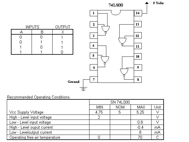
- 7400: Quadruple 2-Input Positive NAND Gates
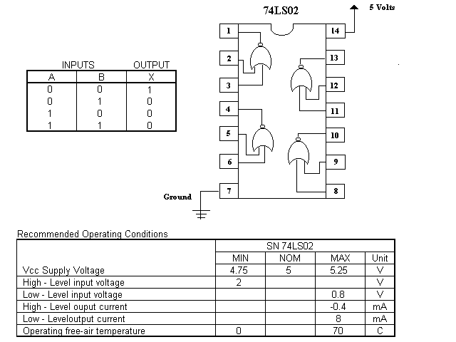
- 7402: Quadruple 2-Input Positive NOR Gates
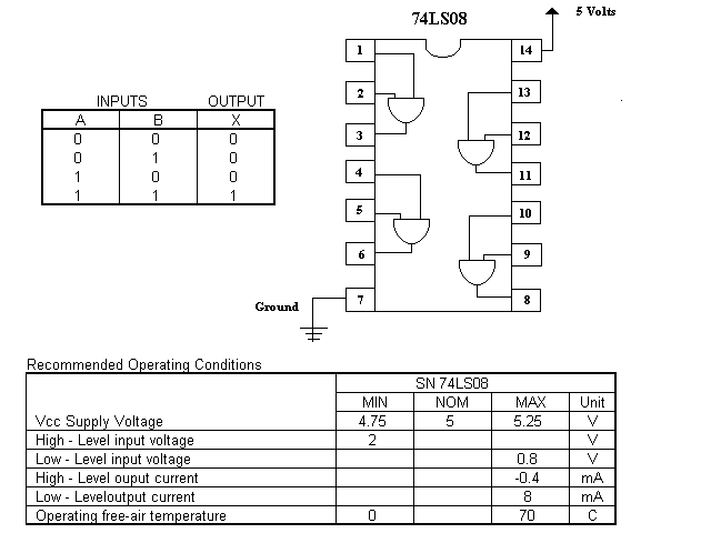
- 7408: Quadruple 2-Input Positive AND Gates
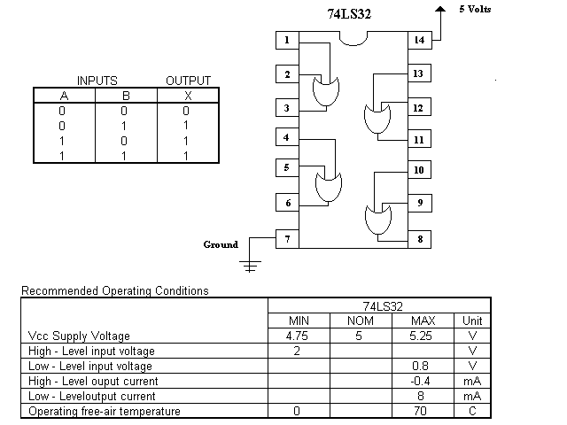
- 7432: Quadruple 2-Input Positive OR Gates
- Laboratory Experiments
- Explore the Operation of the AND gate.
- Look up the TTL part number for a two-input AND gate and obtain
this chip from the lab instructor. Sketch a diagram of the chip
showing which gates inside the chip connect to which pins on the chip.
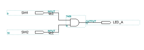
- Connect the inputs of one of the AND gates to the switches on
the D/A Trainer and the output of the AND gate to an LED on the D/A
Trainer. Construct the circuit diagram.
- Verify proper operation of the AND gate for all input
combinations by using the input switches. When the LED is lit, this
indicates a high logic level or 1. When the LED is off, this
indicates a low logic level or 0. Demonstrate this part to the Lab instructor.
- Record the TTL part number and produce a truth table on the
results of 1.3.
- Explore the Operation of the OR gate.
- Look up the TTL part number for a two-input OR gate and obtain
this chip from the lab instructor. Sketch a diagram of the chip
showing which gates inside the chip connect to which pins on the chip.
- Connect the inputs of one of the OR gates to the switches on
the D/A Trainer and the output of the OR gate to an LED on the D/A
Trainer. Construct the circuit diagram.
- Verify proper operation of the OR gate for all input
combinations by using the input switches. When the LED is lit, this
indicates a high logic level or 1. When the LED is off, this
indicates a low logic level or 0. Demonstrate this part to the Lab instructor.
- Record the TTL part number and produce a truth table on the
results of 1.3.
- Explore the Operation of the NAND gate.
- Look up the TTL part number for a two-input NAND gate and obtain
this chip from the lab instructor. Sketch a diagram of the chip
showing which gates inside the chip connect to which pins on the chip.
- Connect the inputs of one of the NAND gates to the switches on
the D/A Trainer and the output of the NAND gate to an LED on the D/A
Trainer. Construct the circuit diagram.
- Verify proper operation of the NAND gate for all input
combinations by using the input switches. When the LED is lit, this
indicates a high logic level or 1. When the LED is off, this
indicates a low logic level or 0. Demonstrate this part to the Lab instructor.
- Record the TTL part number and produce a truth table on the
results of 1.3.
- Explore the Operation of the NOR gate.
- Look up the TTL part number for a two-input NOR gate and obtain
this chip from the lab instructor. Sketch a diagram of the chip
showing which gates inside the chip connect to which pins on the chip.
- Connect the inputs of one of the NOR gates to the switches on
the D/A Trainer and the output of the NOR gate to an LED on the D/A
Trainer. Construct the circuit diagram.
- Verify proper operation of the NOR gate for all input
combinations by using the input switches. When the LED is lit, this
indicates a high logic level or 1. When the LED is off, this
indicates a low logic level or 0. Demonstrate this part to the Lab instructor.
- Record the TTL part number and produce a truth table on the
results of 1.3.
- What level does an unconnected input appear to be (high or low)?
(Hint: Repeat one of the previous operations with one input left
unconnected.) What reasoning did you use to determine your answer?
